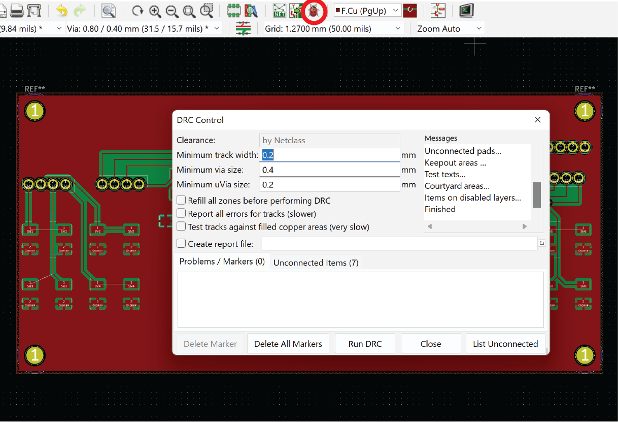
WEEK 6.

ELECTRONICS DESIGN.

March 19, 2022

Programming.

I started by following a tutorial on making a simple pcb design to light up some leds with switches to familiarize with the software and the principles of electronics. In KiCad I started by laying out all the components I need. The basic shortcuts you need to know are 'M' while your mouse is on top of the object you wish to move and then move it to where you want and 'R' to rotate that object.

post-thumb

PCB DESIGN.

post-thumb

1.

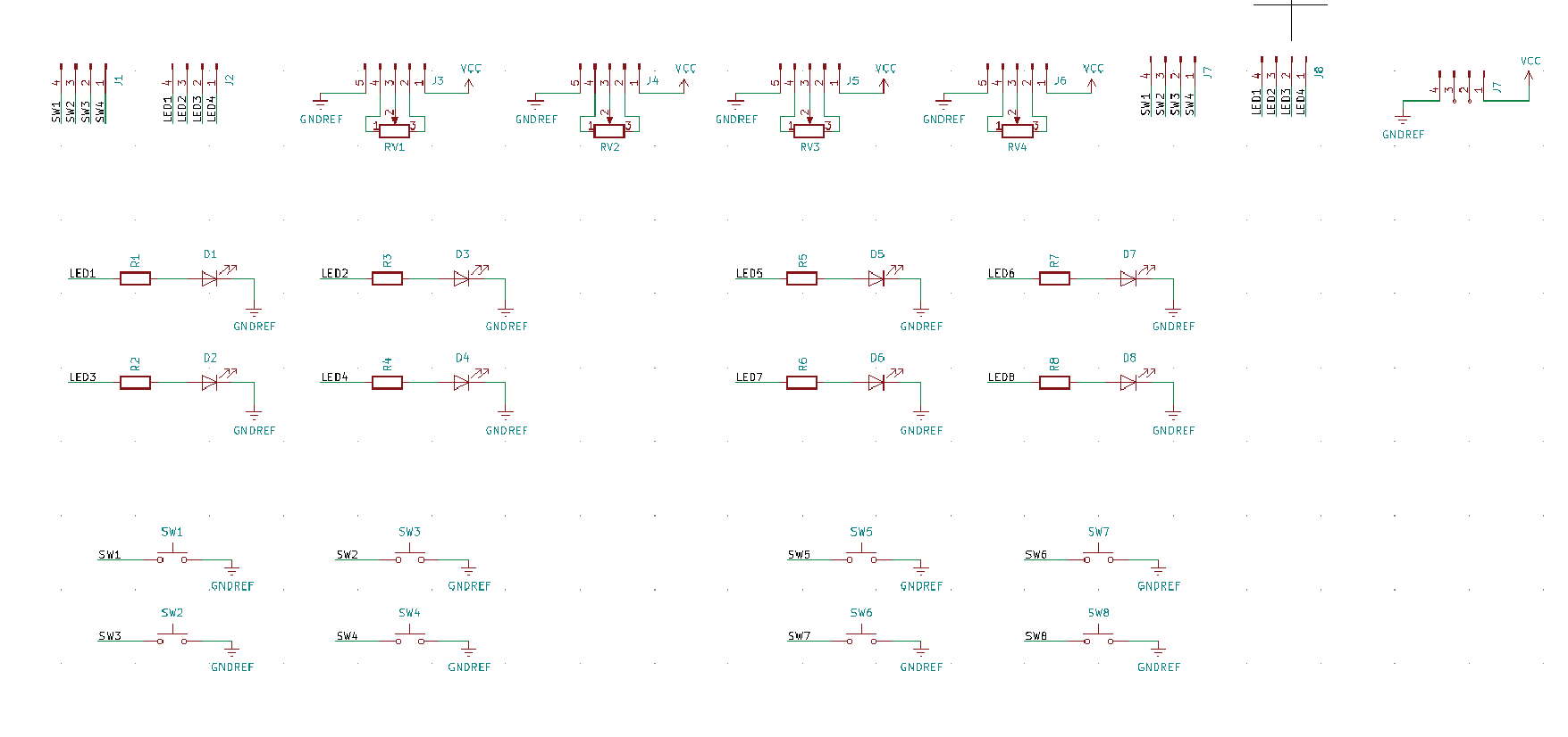
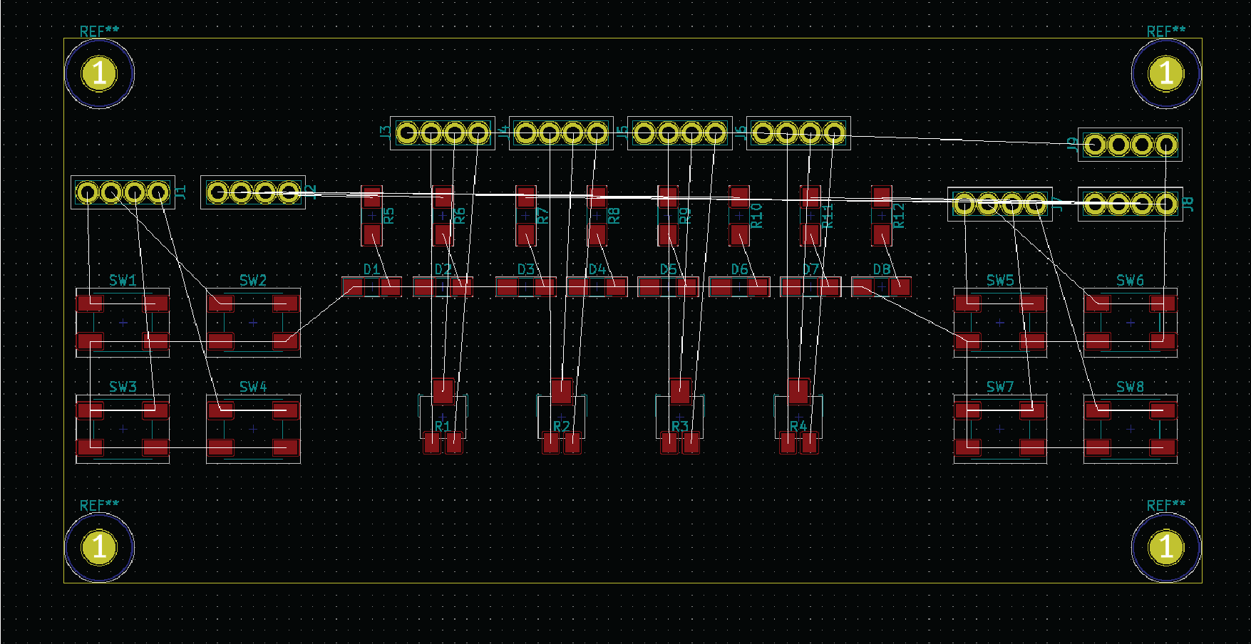
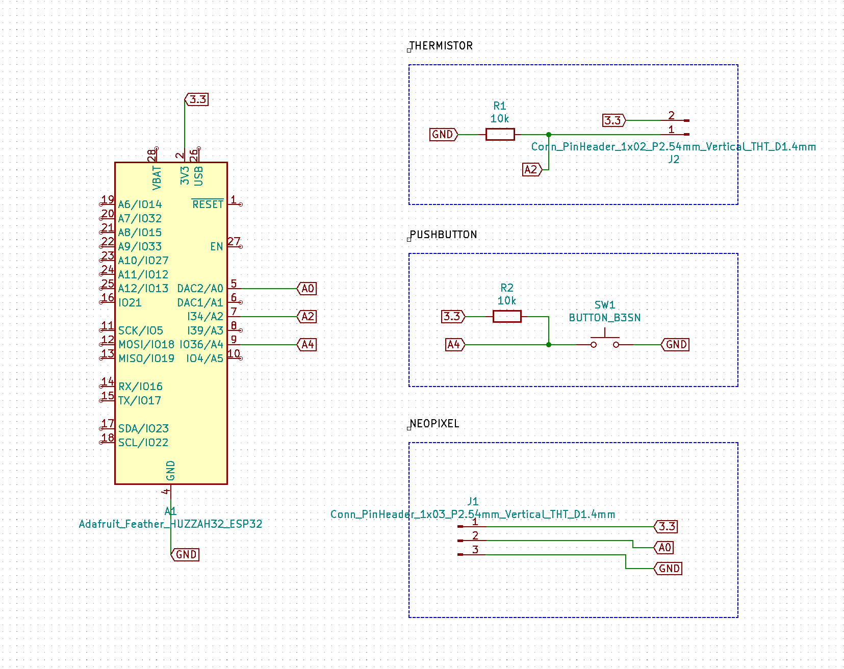
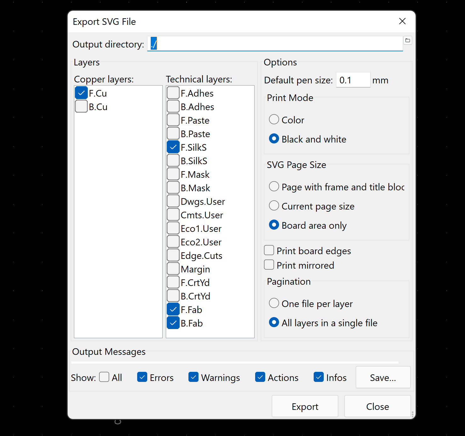
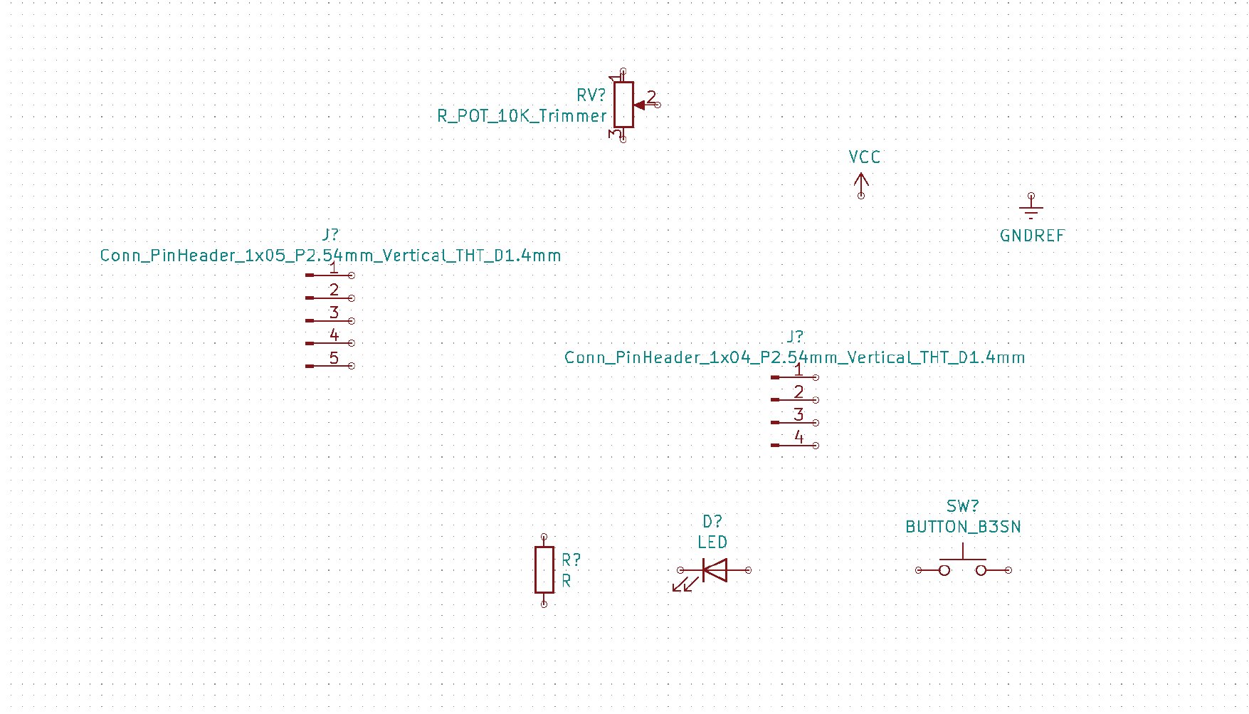
I clicked the annotate symbol in order to give numbers to the components. Afterwards I right clicked in every component to edit the name and untick the visible box so it would only display the letter and number and not all the technical details. Making the layout easier to navigate.

post-thumb

2.

In this image I now have all the components I will need for this pcb. I clicked annotate once again with all the components and made sure the order was correct. Then I created the neural netlist and saved it.

post-thumb

3.

Once you have it you select the icon of the pcb layout editor and it directs you to a new blank page. You open your saved neural netlist and now the components will be laid out.

post-thumb

4.

Once you have all the components laid out it could like kind of messy so you can use CTRL F to find the name of the component and rearrange it.

post-thumb

5.

After organizing everything this is the result I got.

post-thumb

6.

I added 4 mounting holes of 2.5 mm in each corner for the pcb and then I added a graphic line to select the boundary of my piece.

post-thumb

7.

Then I started connecting with wires all the pieces that needed to interconnect.

post-thumb

8.

Some wires were intersecting with others so what we have to do is use the 'V' or right click then place through via in order to create sort of bridges.

post-thumb

9.

After connecting everything I created a filled zone for the ground and duplicated it, pasted it in the same place and then edited and changed it for the backface layer.

post-thumb

10.

Before exporting be sure to check for errors in the Design Rule Check button.

post-thumb

11.

Now we create the plot files and we select the layers we want to export.

post-thumb

12.

After creating the plot files exporting the different layers we generate the drill files.

post-thumb

13.

You can check your pcb before exporting with the view-3d viewer.

After this I decided to try to design my own PCB. At the moment I'm working with my design collaborative SlowLab on designing a Solar Oven. We want to add a thermometer so we can know the temperature reached by the oven. We first wired the electronics needed. In this case this is what we used and how we connected everything.

post-thumb

We needed an NTC thermistor to measure temperature, a push button that would detect when to start collecting the data and the neopixels that would display different colors depending on the temperature it reached. We connected all the electronics first to make sure it worked. After that we passed the schematics to KiCad.

post-thumb

1.

We searched for the components on the fab library and placed them on the sketch. We organized them into boxes so we would have a clearer view of what was going on. We created labels to indicate where the connections would go. After we were happy with the connections we generated the netlist and opened the pcb design.

post-thumb

2.

We changed some parameters for the pcb design.

post-thumb

3.

After importing the netlist we organized the components in a neat way so we could occupy the least of space and the connections would be able to work properly. This part was very tricky because some connections were interrumpted by others so we had to sort of solve the puzzle in order to find the best suitable arrangement for all the connections.

post-thumb

4.

After creating the final wiring, we exported as svg and selected the layers we wanted to export, in this case we also selected Front Fab and all layers in a single file.

post-thumb

5.

Once we had our file exported we opened it on illustrator and separated by layers the drills, outcut, board and traces.

post-thumb

6.

We went into the website mods project and right clicked programs/open/pcb ce and then imported our png files from the illustrator file. One for the drills, another for traces and last one for cut. The parameters that we used were: 1.Traces-speed 3 and 1/64 bit. 2.Drills-speed 3 and 1/32 bit. 3.Outline cut- speed 1.5 and 1/32 bit.

OTHER ASSIGNMENTS